The Neurograin project targets the development of next generation neurotechnology for very large-scale recording and stimulation of distributed brain areas through a wirelessly networked ensemble of completely implantable microdevices (Figure 1).
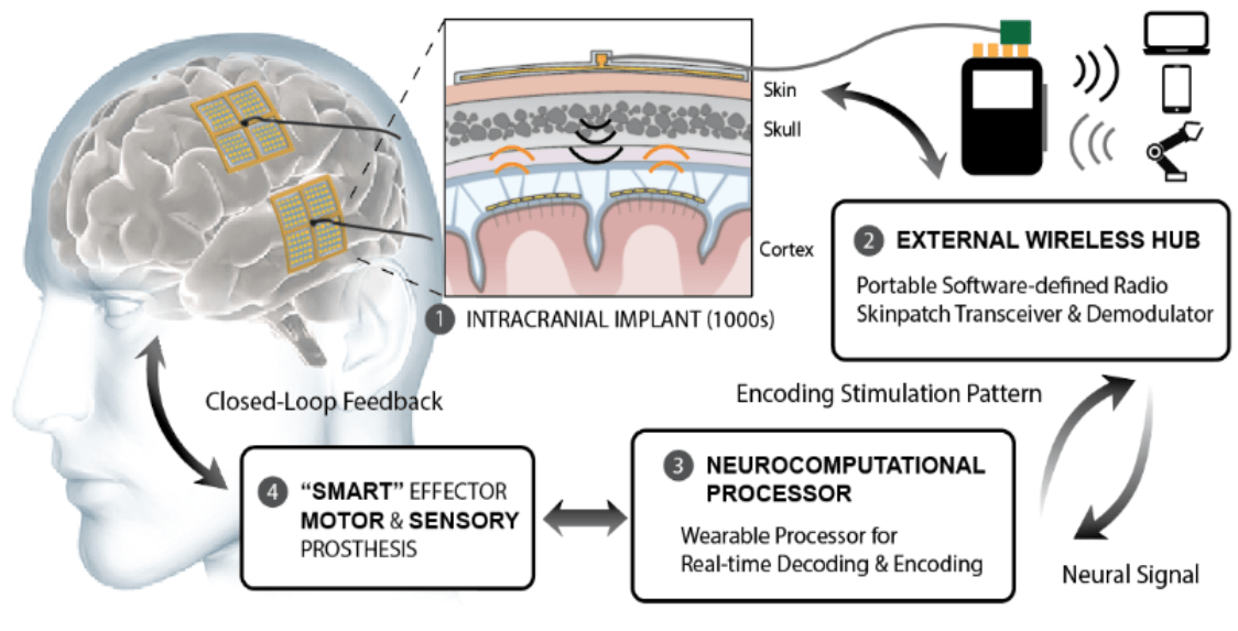
We have developed sub-millimeter, hermetically sealed implants (implant volume <0.01 mm3) integrating microchiplets with capabilities for neural recording and electrical microstimulation, wireless power delivery and bidirectional networked telemetry. We envision the deployment of these devices across the brain in numbers ranging up to thousands. Active areas of research and development in this neurotechnology arena are:
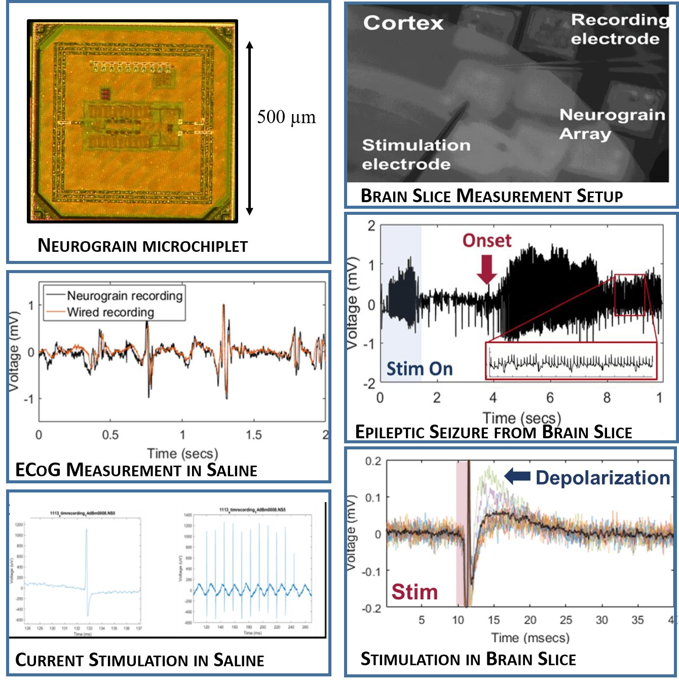
1. Low-power, Low-noise custom microelectronic circuit design: We are using advanced CMOS process technologies for development of high-performance, low-noise, ultra-low-power integrated circuit solutions for a completely wireless neural interface implementation Current prototype devices measure 500 µm x 500 µm, and enable 500 Hz ECoG band measurement as well as biphasic current-mode electrical microstimulation up to 25 µA. Additionally, each individually addressable microchiplet integrates RF circuitry for high-efficiency energy harvesting and networked telecommunications (Figure 2).
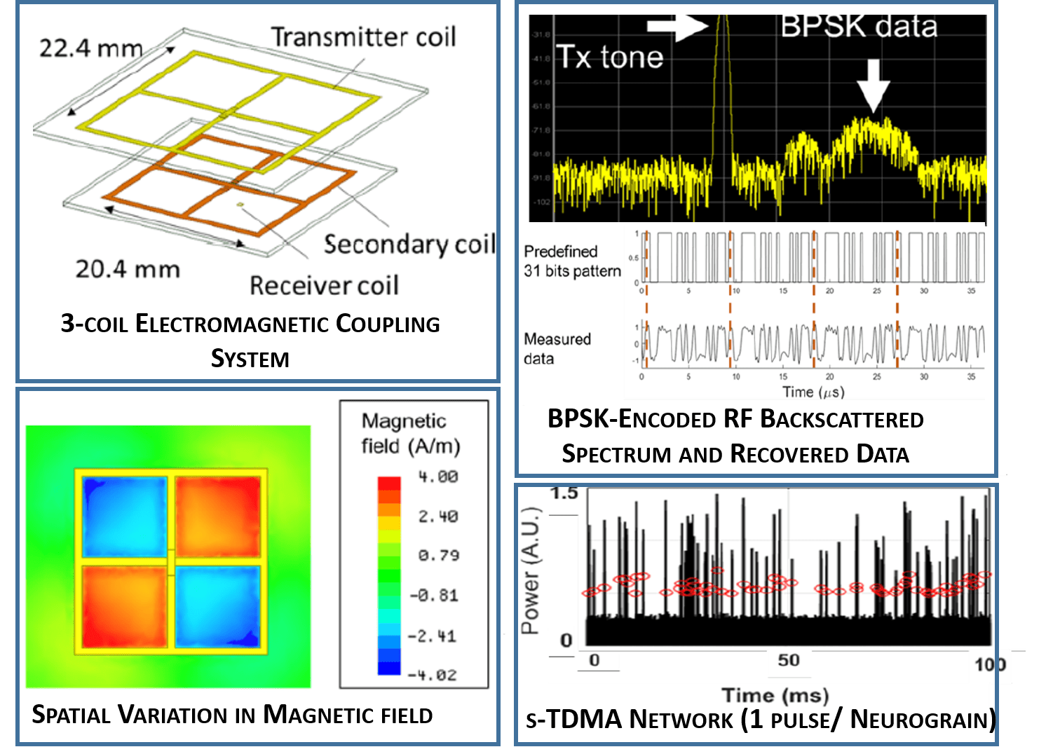
2. Wireless Energy Transfer and Telecommunications: We utilize near-field RF inductive coupling for transcutaneous wireless power delivery to the implanted microdevices; our current approach offers an order of magnitude improvement in energy harvesting capabilities over standard approaches. We use a single-channel approach for power delivery and bidirectional communication relying on a combination of carrier modulation (ASK-PWM) and synchronized time-domain multiple access (s-TDMA) RF backscatter and are working to develop an optimized electromagnetic framework for energy delivery and synchronized, bidirectional, networked wireless telecommunications with high-efficiency data links in the 10s of Mbps range.
3. Portable Embedded System solutions for real-time Neurocomputational processing: We are implementing a system architecture enabling real-time coordination and management of the implanted Neurograin devices by a wearable external telemetry hub leveraging Software-Defined-Radio (SDR) and Ultra-High-Performance Field Programmable Gate Array (FPGA) technologies. The latter is also anticipated to relay data to high-performance neural processors in-situ and/or on the cloud for neural decoding/encoding facilitating closed-loop brain-computer interface control.
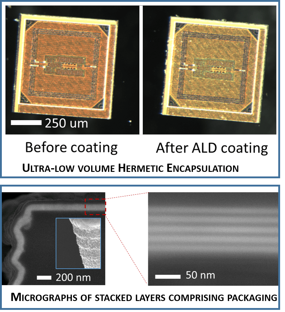
4. High-throughput hermetic packaging of microdevices: We have developed a stacked thin-film (~ 100 nm) conformal coating approach to hermetically encapsulate Neurograin microdevices. The microchiplets are batch processing using Atomic Layer Deposition (ALD) techniques enabling the production of a biocompatible implants with less than 1% increment in overall device volume between unpackaged and packaged devices ( Figure 4).